A Closer Look at the BMPCC 6K and 6K Pro Thermal Architecture and Component Longevity
An engineering review of thermal management in the BMPCC 6K and 6K Pro, and what running a Sony IMX571 stills sensor continuously means for its longevity.
Engineering Review: A Closer Look at the BMPCC 6K and 6K Pro Thermal Architecture and Component Longevity
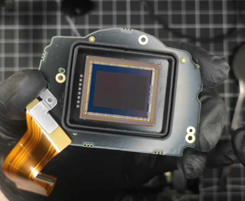
Sony IMX571BQR sensor
'None of this changes what the camera fundamentally is: a consumer stills sensor, run continuously in a role its own manufacturer declines to warrant, inside a plastic body that cannot shed heat outward, cooled by a single fan that reaches the sensor last'.
The thermal management system of the Blackmagic Pocket Cinema Camera (BMPCC) 6K and 6K Pro lines is a frequent topic of discussion among filmmakers due to the heat output through the exhaust port. While these cameras are highly capable tools for recording high-bitrate 6K BRAW, an analysis of their internal layout reveals a series of complex engineering choices. To balance form factor, weight, acoustic noise, and price point, the design incorporates distinct compromises that directly impact how heat moves away from the core components.
Understanding these thermodynamic mechanics can help operators better manage their hardware and optimise their camera's long-term performance.
Update: since first publishing this, I have had a 6K Pro stripped to the mainboard on the bench and identified the image sensor. Knowing exactly which part is being cooled sharpens several of the points below, and puts one of them on a numerical footing.
The Sensor: A Sony IMX571BQR
- The Part: The image sensor is a Sony IMX571BQR, identified from the die marking. It is a back-illuminated Type 1.8 CMOS device, 6244 x 4168 active pixels on a 3.76 micron pitch, in a 184-pin LGA package. Blackmagic's published effective sensor size of 23.10mm x 12.99mm divides out to that same 3.76 micron pitch, which is consistent, though Sony use that pitch across a family of parts, so it narrows the field rather than closing it.
- A Stills Sensor, Cropped to Cinema: The camera records 6144 x 3456, which is roughly 98% of the sensor's available width but only 83% of its height. This is a 3:2 stills sensor windowed down to a 16:9 cinema frame.
- Sony Decline to Warrant It: The product brief states plainly that the device is designed for consumer digital still cameras, and that for any other application Sony "does not guarantee the quality and reliability of this product."
That restriction is a commercial qualification tier rather than a technical verdict. The same document advertises 4K movie readout and windowed modes running past a thousand frames per second, so the video capability was designed in deliberately. What it does mean is that consumer-grade screening, no long-term availability commitment, and characteristics quoted at a 60 degree C junction temperature are the terms Blackmagic had to build around. They characterise the part themselves, and they carry the risk themselves.
That raises the stakes for everything below rather than settling them. A device whose manufacturer explicitly declines to warrant it for continuous duty is precisely the device you would want given the most thermal margin available. The sections that follow describe a design that gives it comparatively little.
1. Outer Shell Composition and Internal Frame
- The Architecture: Aside from a pressed steel internal structural chassis, the outer camera body is constructed from a carbon-fibre-reinforced polycarbonate composite (Plastic). This material matrix consists of roughly 10% to 30% carbon fibre, with the remaining bulk being industrial plastic.
- The Thermal Dynamic: While the addition of carbon fibre can improve structural rigidity and reduce weight, it does not alter the fundamental thermal insulating properties of the plastic base. Unlike the full magnesium or aluminium alloy housings found on high-end cinema gear (or an iPhone!)—which act as large passive external heatsinks—this composite shell effectively traps heat inside the camera body.
- The Impact: Because the outer shell cannot efficiently radiate heat outward into the environment, the internal pressed steel frame and active airflow path are forced to handle effectively all of the camera's thermal dissipation workload.
2. The Single-Chamber Shared Airflow Layout
- The Architecture: The camera utilises a single internal blower fan designed to clear heat from both the high-draw FPGA SoC (system on a chip) and the image sensor assembly.
- The Thermal Dynamic: Because the fan draws air across the mainboard electronics first, the airflow is already carrying significant thermal energy by the time it reaches the sensor heatsink.
- The Impact: This shared pipeline places a heavier workload on the sensor's Thermoelectric Cooler (Peltier element). A Peltier element is a heat pump rather than a heat sink. That distinction matters in two directions. It can drive the sensor below the temperature of its surroundings, which no passive path can achieve at any size. But it does so by pumping heat to its hot side and adding its own electrical input power to the total, so more heat must ultimately be rejected from the camera than the sensor produced in the first place. It also pays a compounding penalty: its efficiency falls as the temperature difference across it rises. Delivering pre-warmed air to that hot side therefore costs twice over: it raises the temperature difference the element must sustain, while reducing the rate at which the heat it has already moved can leave.
- The Consequence: The component with the most to gain from running cold is the one placed at the far end of the duct, downstream of everything else.
- The 6K Pro Factor: While the 6K Pro version introduces excellent quality-of-life upgrades like motorised internal ND filters and a brighter 1500-nit HDR tilt screen, the underlying cooling path remains identical. The added power draw of the 1500-nit display and the thermal bulk of the internal NP-F570 batteries place an even higher collective heat load on this shared single-fan wind tunnel.
3. The sensor heatsink Pedestal Dimension Constraints
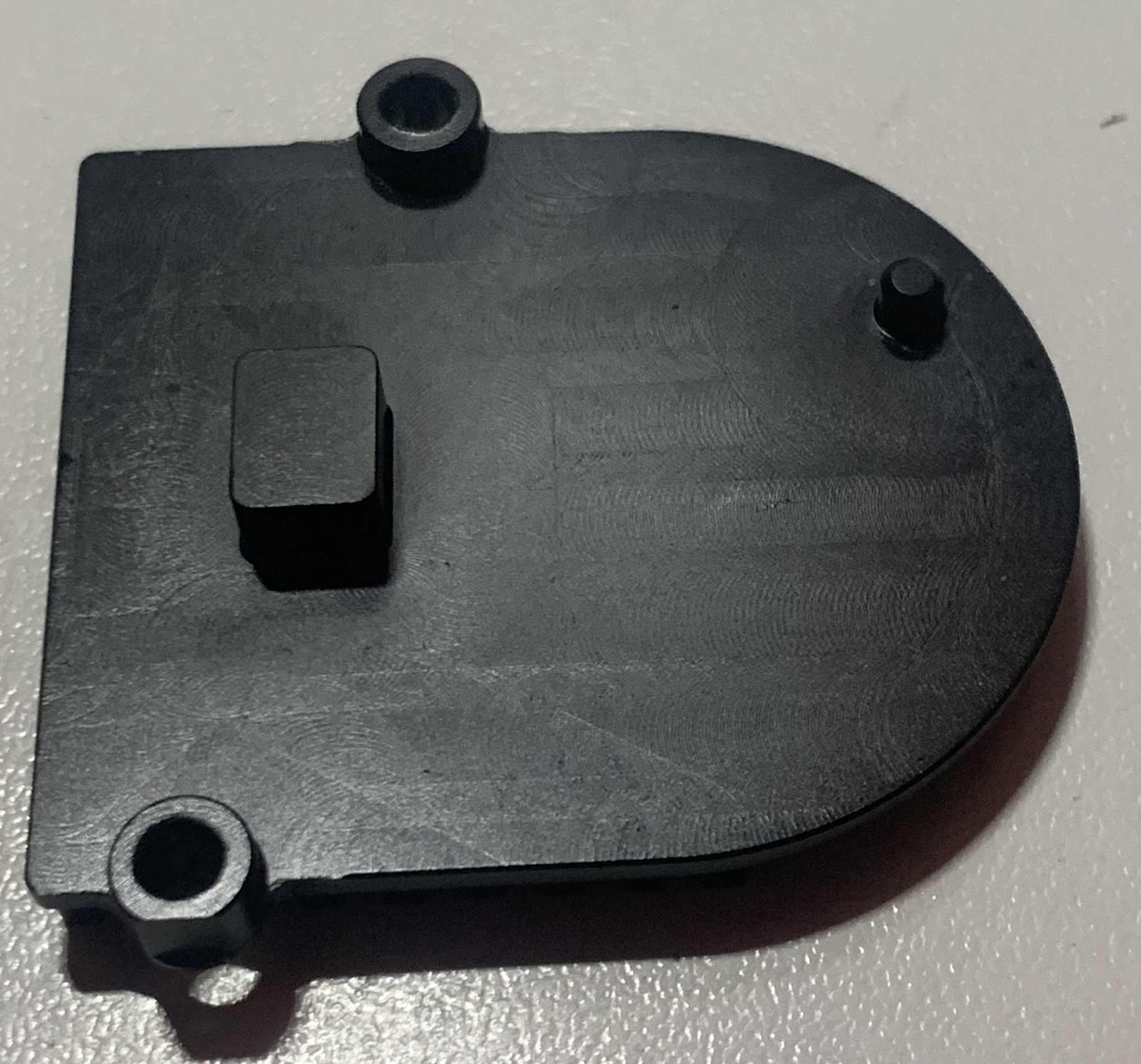
- The Architecture: Thermal energy travels from the sensor assembly to the main finned heatsink via a distinct metal protrusion measuring approximately 9 x 6.65 x 6mm.
- The Thermal Dynamic: Choking a heat path down to a restricted cross-section naturally introduces higher thermal resistance compared to a completely flush, full-surface contact plate.
- The Load It Actually Carries: With a Peltier element in the path, this pedestal is not merely conducting away the sensor's own dissipation. Everything the Peltier pumps out of the sensor, plus the electrical power the Peltier itself consumes, has to leave through that same restricted cross-section. The load crossing it is therefore strictly greater than the sensor alone would impose.
The Engineering Trade-off: Due to the design of the sensor pcb this pedestal is a structural necessity. It acts as a physical riser, elevating the bulky cooling fins safely above the delicate capacitors, resistors, and ribbon cable connectors populated on the surrounding sensor circuit board.
Having now had that board out, the constraint is real and tighter than it looks from the outside. The sensor sits closely surrounded by its own power conditioning, including two Texas Instruments TPS7A87 dual low-noise regulators, chosen for 3.8 microvolts RMS of output noise because supply noise on a sensor rail lands visibly in the picture. Those components have to be exactly where they are, immediately adjacent to the sensor. A full-surface contact plate would foul them.
4. Surface Finish and Interface Mechanics
- The Architecture: The entire aluminium heatsink features a black anodized finish, including the flat mating surface on the contact pedestal.
- The Thermal Dynamic: Anodising is beneficial on the cooling fins; the resulting black oxide finish raises surface emissivity substantially over bare metal, improving radiative transfer inside the air channel. However, aluminium oxide has significantly lower thermal conductivity (~30 W/mK) than raw aluminium (~200 W/mK).
- The Impact: Leaving the anodised layer intact on the exact point of physical contact introduces a barrier right at the primary thermal junction, limiting the rate of direct conductive heat transfer. The two cases differ because of area. The oxide layer is only microns thick, so on the fins its resistance is negligible: the heat is spread across a large surface and the flux through any part of it is low. At the contact face the entire load funnels through roughly 60 square millimetres, so the flux density is enormous and the same thin layer becomes a real obstacle.
- Why It Compounds Here: On a Peltier-cooled sensor, resistance at this junction is not simply a slower path. It raises the hot-side temperature, which increases the difference the Peltier works across, which lowers its efficiency, which increases the heat it must reject through the very same junction.
Long-Term Hardware Considerations: Thermal Stress
Sustained exposure to localised thermal energy can accelerate the natural ageing process of microelectronics through two well-documented physical phenomena:
- Thermal Expansion Strain: Different materials (the silicon die, solder points, and fibreglass PCB substrate) expand and contract at different rates. Large temperature swings from repeatedly powering the camera on and off generate mechanical stress across the solder joints over time, which can eventually lead to intermittent connectivity issues.
- Sensor Crystal Lattice Stress: Operating semiconductor sensors at elevated temperatures over multiple years gradually increases defect density in the silicon, and with it the pixel leakage known as dark current. This degradation is permanent and cumulative rather than something that clears on cooling down.
The thermal expansion point is not merely theoretical. On the board currently open on my bench, the USB-C connector's through-hole joints show poor wetting from the factory. Joints that begin marginal are precisely the ones that years of thermal cycling eventually find.
What the Sensor's Own Numbers Tell Us
Identifying the sensor allows the second point to be tested rather than asserted, because the IMX571 has been characterised in unusual depth by astrophotography camera manufacturers, who cool it thermoelectrically and publish the results.
- Dark current: approximately 0.0005 electrons per pixel per second at -20 C
- Read noise: 1.2 electrons at high gain, 3.6 electrons at low gain
- Full well capacity: above 50,000 electrons
Two of those figures answer a question the original article raised. Full well capacity divided by read noise sets the ceiling on dynamic range: above 50,000 electrons against a 1.2 electron floor is a ratio of roughly 40,000 to one, or about 15 stops. Blackmagic quote 13 stops for the camera, so the claim sits comfortably inside what the silicon can deliver, with headroom for the losses of real optics and real processing.
Dark current in silicon roughly doubles every 6 to 7 degrees C. Taking the measured figure at -20 C up to the 60 degree C junction temperature at which Sony quote the part gives about twelve doublings, landing somewhere near 2.5 electrons per pixel per second.
At a 1/50th second exposure, that amounts to roughly five hundredths of an electron per pixel, against a read noise floor of 1.2 electrons. It is swamped, by a factor of more than twenty.
This is worth stating plainly, because it corrects a widely held assumption, and one I made myself in the original version of this article. Uniform dark current is not what threatens image quality in a cinema camera. At exposure times measured in hundredths of a second it is negligible even with the sensor running hot, and it would remain negligible even if ageing multiplied it several times over. The reason astrophotographers must hold this same sensor at -20 C is that they integrate for minutes at a time; at those exposures the identical leakage accumulates into a visible fog. Same silicon, same physics, entirely different regime.
What survives the arithmetic are the effects that are not uniform, and these are the ones the cooling system genuinely earns its place against:
- Hot pixels: individual defective pixels leak orders of magnitude faster than the average, which makes them visible even at short exposures. They accumulate permanently with thermal ageing, and this is the mechanism by which a sensor genuinely degrades over years of hot operation. It is also why cameras carry defect maps at all.
- Fixed pattern noise: a structured, non-random offset that rises with temperature. Because it is correlated rather than random, it is not averaged away by a short exposure in the way that shot noise is, and the eye is unusually good at seeing it.
- Mechanical fatigue: the thermal expansion strain described above, which is driven by temperature swings rather than by absolute temperature.
So the case for cooling this sensor is sound, but it is not the case usually given for it. The Peltier is not there to hold down dark current during a take. It is there to limit the permanent accumulation of defects across the working life of the camera, and to suppress the structured noise that short exposures cannot average away.
It is also why the sensor is given a Peltier when the FPGA makes do with airflow alone. The FPGA merely has to stay below its operating limit; beneath that threshold, further cooling buys nothing. The sensor has no such threshold. Its degradation rate is a continuous function of temperature, so every degree removed returns something, and that is what justifies the cost, power draw and complexity of a Peltier stage.
Technical Optimisation Options for Enthusiasts
For users comfortable with hardware modifications or out-of-warranty repairs, the thermal transfer rate at the pedestal junction can be optimised manually:
- Precision Lapping: Gently sanding only the flat 9 x 6.65mm contact face with ultra-fine grit wet sandpaper (1000–2000 grit) removes the lower-conductivity anodised layer to expose the raw aluminium beneath. Lap the contact face only. The anodising is doing useful work on the fins and should be left intact there.
- Interface Upgrade: Reassembling the bracket with a premium, high-conductivity thermal paste ensures maximum surface contact, bypassing the factory interface limitations without altering the camera's active fan profiles.
Both modifications act on the same junction, and on a Peltier-cooled sensor that junction is the leverage point: reducing its resistance lowers the hot-side temperature, which raises the efficiency of the Peltier working across it.
None of this changes what the camera fundamentally is: a consumer stills sensor, run continuously in a role its own manufacturer declines to warrant, inside a plastic body that cannot shed heat outward, cooled by a single fan that reaches the sensor last. That it performs as well as it does is a genuinely creditable piece of engineering. But the margin is thinner than on a magnesium-bodied cinema camera, and on this design the margin that does exist is well worth protecting.